
Over the weekend, IEEE published a guest article from two MIT researchers working with DARPA to develop a LiDAR-on-a-chip. (For those in the know, the technology is called “solid state” LiDAR).
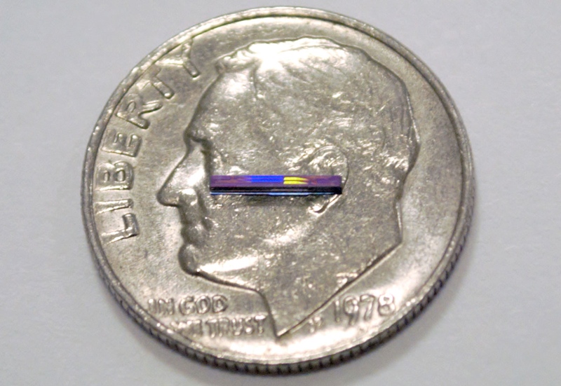
The news is spreading around the internet fast, thanks in no small part to a picture that shows MIT’s LiDAR chip on a dime, a thin line spreading from Franklin D. Roosevelt’s eye to his ear. It’s seriously small—and researchers believe the technology will be commercially available within a few years at a cost of only $10 per LiDAR chip.
Here’s everything you need to know. Including the chip’s specs, applications, limitations, and what it means for commercial and consumer LiDAR.
Basic details:
- The LiDAR chips are produced on 300-millimeter wafers in commercial CMOS foundries (or: the same kind of manufacturing facilities producing the microchip in your computer).
- LiDAR on a chip is “orders of magnitude smaller, lighter, and cheaper than lidar systems available on the market today.”
- Researchers expect that once these foundries are producing these chips in the millions (!), they will reach a cost of only $10 per LiDAR.
- Because the devices include no moving parts, they will be 1,000 times faster than the current mechanical systems, which use a mirror to direct the beam.
- For more on the mechanics of solid-state LiDAR, check out my explainer article here.
Specs:
- The beam covers a spread of only 51° degrees.
- The range is currently limited to 5 meters.
- Resolution is 3 centimeters at a 2-meter range.
Improvements are coming soon:
- Researchers hope to achieve a spread of of 100° and a range of 10 meters within a year.
- There is a “clear development path toward lidar on a chip technology that can reach 100 meters, with the possibility of going even farther.”
Commercial applications:
- The devices are designed for robotics and autonomous vehicle applications
- BUT, the authors report “promising results in creating very-large scale arrays for lidar applications,” meaning that these sensors could be combined to create a larger LiDAR beam.
- As a result, we can reasonably expect to see a commercial handheld LiDAR device built with this technology some day, costing somewhere in the range of hundreds of dollars rather than thousands. Within the near future, your cell phone may include a LiDAR chip.
- Imagine using a commercial device built with the LiDAR on a chip technology to scan an item for Q&A, or a valve for replacement, or a room for documentation. LiDAR on a chip will bring LiDAR into applications where we’ve been using structured light or photogrammetry.
- For more on the commercial applications of solid-state LiDAR, see SPAR 3D’s article here.
This is some crazy futuristic tech
These on-chip lidar systems, the article explains, could “even be placed in the fingers of a robot to see what it is grasping because of their high resolution, small form factor, and low cost.”
Put more simply, we are approaching a huge disruption of LiDAR technology as we know it. A sensor that is so cheap, so small, and with different capabilities than current LiDAR systems is sure to bring big changes and lots of new applications–and it’s coming soon.