
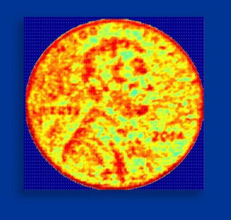
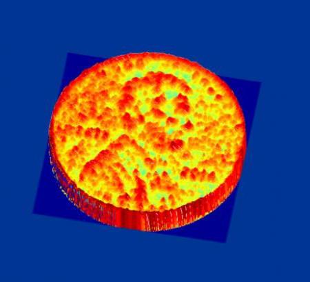
A 3D image of a penny, produced by the new NCI chip. Credit: Ali Hajimiri/Caltech
LiDAR used to fill a van–today you can buy a device that fits in your hand. And it just got even smaller.
Last month, researchers at Caltech published a paper describing an extremely compact 3D-imaging technology. It’s called the nanophotonic coherent imager (NCI) and it is made up of individual LiDAR devices, each one a silicon chip about a hundred microns in size. Despite these incredible numbers, Caltech’s website says that the coherent imager device is capable of “the highest depth-measurement accuracy of any such nanophotonic 3-D imaging device,” putting the accuracy squarely in the micron range.
Ali Hajimiri, professor of Electrical Engineering at Caltech and head of the lab where the NCI was developed, explains the benefits of a 3D-imaging device comprised of tiny LiDAR chips. Using such a device, he says, you can “simultaneously image different parts of an object or scene without the need for any mechanical movements within the imager.”
This means you can also image a scene without moving the device, or moving yourself. You operate it like a camera (this is why the researchers call the chips “camera chips”) but it works like LiDAR.
How did the team make the LiDAR devices so small? The details are very technical, but here’s the gist if you don’t feel like digging in: by exploiting the optical concept of coherence, the team was able to alter silicon chips to measure the way objects interfere with the frequency and wavelength of light. This enables the chips to gather depth information about those objects. Silicon chips, as we know, can be made very small. (For a more complete explanation, including technical details, check out Caltech’s statement.)
It’s important to remember that the technology is in the proof of concept phase, which means you probably won’t be seeing it in your cell phone for a number of years. And since the number of these tiny LiDAR chips they’re able to incorporate in a single 3D-imager is still really, really small, the 3-D images it takes are small too. For now, the biggest 3D images they can take in a single shot is 16 pixels in size. That’s small enough that they had to develop some clever processing to image a full US penny. (Once they figured it out, they got an image with 15 micron depth resolution and 50 micron lateral resolution from about half a meter away.)
Is it scalable? Hajimiri says yes. The technology could be scaled up to include hundreds of thousands of tiny LiDAR chips and capture hundreds of thousands of pixels. “One day, by creating such a vast array of these tiny LiDARs,” the Caltech website explains dreamily, “the imager could be applied to a broad range of applications from very precise 3-D scanning and printing to helping driverless cars avoid collisions to improving motion sensitivity in superfine human machine interfaces, where the slightest movement of a patient’s eyes and the most minute changes in a patient’s heartbeat can be detected on the fly.”
Being so small, accurate, and cheap, these tiny LiDAR devices could open a whole new raft of uses for LiDAR. Hajimiri hopes these cost reductions will enable “thousands of new uses” for the technology by putting them into personal devices. But why stop there? It could also put LiDAR almost anywhere you could imagine. Around your facility to constantly gather scans and compare them against the existing model, for instance. That would be true real-time change detection.
For more technical detail on how this device works, check out Caltech’s statement. For even more technical detail, see Hajimiri’s paper “Nanophotonic Coherent Imager,” co-authored with Firooz Aflatouni, Behrooz Abiri, and Angad Rekhi.