
We repeat it so often that it’s becoming cliché: The demand for autonomous vehicles means unprecedented amounts of money are flowing into lidar development, and that’s bringing new, lower-cost, and potentially groundbreaking technologies to the market. It’s disrupting our cozy little 3D-scanning industry.
Ouster is a great case study for this phenomenon. In January, the company announced a lidar sensor that took on the incumbent automotive lidar manufacturer by offering 64-channel scanning at 1/6 the cost. Next, the company released a $3,500 16-channel lidar, and then a firmware upgrade that enabled its flagship lidar to gather 2D signal-intensity images and ambient images in real time, without a camera. It’s worth noting that Ouster has designed its lidar to be used for vehicle-, drone-, and robot-based mapping, not just autonomous navigation.
And these hardware releases looks like they could be just the start Ouster’s plan. In a recent interview and a blog post, CEO and co-founder Angus Pacala went deep on his company’s technology and laid out a few future possibilities enabled by its “radically different” approach to lidar.
A (different) solid-state lidar
The first factor that differentiates Ouster’s lidar is that it’s based on solid-state technology. That is, where most existing high-performance lidar for the automotive market (or for other markets) are built with thousands of little electronic parts, Ouster’s lidar replaced virtually all of those parts with two silicon-based microchips. This approach is miniaturizing the lidar sensor just it once helped shrink the room-sized computer down to a slick bar of glass you can slip into your pocket. (My congratulations to whomever at Ouster wrote the subheading to Pacala’s blog: “silicon eats industries. Lidar is next.”)
Still, a solid-state, automotive-mounted lidar is only somewhat notable in 2018, considering that there are a number of companies publicizing their own solid-state sensors in various stages of completion. However, Ouster sets itself apart again, because its technology works on different principles than virtually every other solid-state solution out there. That’s because Ouster tech uses a unique combination of two custom chips: one vertical cavity surface emitting laser (VCSEL) chip for firing the lasers, and one photon avalanche diode (SPAD) chip for detecting the lasers when they bounce back. Put these two chips together, and you get a “multi-beam flash lidar.”
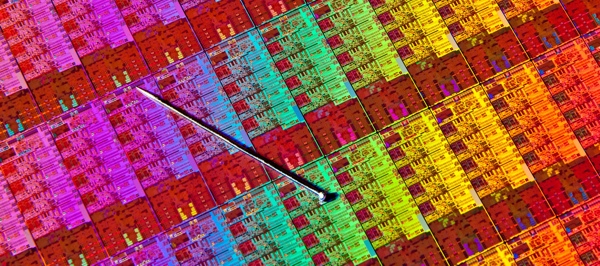
Silicon wafers
Hold up, what is multi-beam flash lidar?
A quick explanation before we move on. In his blog post, Pacala explains that “flash” refers to the idea that “every pixel in the sensor is illuminated by the laser and actively collecting light simultaneously, like a camera with flash.” Put another way, each pixel of the sensor is sending and receiving laser signals at the same time.
Pacala is careful to note that his flash lidar differs from conventional flash lidar (this shouldn’t surprise you, at this point). Traditional flash lidar uses “flood” illumination, which sends out a flood of light, some of which is wasted on parts of the scene where the detectors don’t measure. In contrast, Pacala says, Ouster’s solution illuminates the scene “with precision points of light,” or multiple beams.
What is a VSCEL, and what’s the big deal?
The simplest way to explain the VCSEL is to contrast it against other solid-state laser technologies.
Most solid-state lidars use edge emitters. Ars Technica describes these as “emitting light in the plane of the [silicon]wafer—which means the wafer needs to be cut open to expose the laser’s emission surface.” That makes it hard to build dense arrays of lasers, which is crucial if you want to get high resolution in a small package. The VCSEL, like Ouster uses, “emit[s]light perpendicular to the surface of the wafer. That means there’s no need to cut the wafer in any particular spot for the laser to be functional. And that, in turn, makes building dense arrays of VCSELs much easier.”
Ouster has packed 64 lasers into the single custom VCSEL chip used in its OM-1 lidar, which is about the size a grain of rice. One expert interviewed by Ars speculated that it could be possible to fit millions of lasers on a single chip, just as Intel has done with billions of transistors.
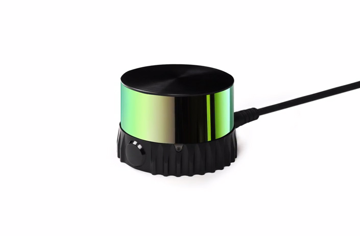
Ouster’s OS-1 lidar
Pacala, for his part, believes that VCSEL arrays could very well develop along similar lines as the digital camera sensor, which has seen designers continuously “pack more pixels in the same space” over the years. He says that Ouster is “going to be able to double, quadruple, 10x the resolution, without any change [in size or cost].”
The VCSEL has a bunch of other benefits. In his blog post, Pacala says that they are smaller, lighter, more durable, faster, simpler to make, and more power efficient than existing laser technologies. They also cost an order of magnitude less. Perhaps most importantly, he believes the technology is on a Moore’s Law-esque trajectory because VCSELs are not only being developed for commercial applications, but also widely used in consumer technology like smartphone cameras and computer mice. That means huge improvements to performance, volume, and cost are coming in the future as hundreds of billions of these chips are built.
And SPADs?
A single-photon avalanche diode is a low noise detector that is sensitive enough to pick up a single photon (as the name indicates). When you think of single-photon lidar, you probably imagine the giant devices that hang off of airplanes for extremely wide area mapping, but SPADs offer a lot of advantages for smaller, ground-based lidar, too.
In his blog post, Pacala focuses most energy on the benefits to be gained from the SPAD’s potential for on-chip processing. He writes that Ouster has built SPADs directly into a semiconductor wafer, which enabled them to incorporate “massive amounts of signal processing” on the silicon “right next to the detectors.”
Essentially, that makes each chip a hybrid of a laser detector and a processor. The one in the OS-1 64-channel lidar counts and stores one trillion photons per second to its memory, and includes processing signal logic to handle over 100 billion operations per second. As anyone who works with 3D data knows, processing requirements are only going to increase in the future, so this kind of integrated chip could turn out to be very useful.
Pacala estimates that these SPAD detectors are going to improve about as quickly as the VCSELs they’re paired with. The SPADs we’re working with, he says, are currently about 2-5% efficient. They will soon hit 20-30% efficiency, and may one day scrape out 80% efficiency. This “makes an OS-1 with 640 lines of resolution not just possible, but extremely likely.”
(What I’ve outlined above is fairly surface level compared to Pacala’s blog, which I recommend you read if you’re interested in more technical detail. He also includes a bunch of information about why Ouster selected an uncommon wavelength for their lasers, and the benefits that wavelength brings.)
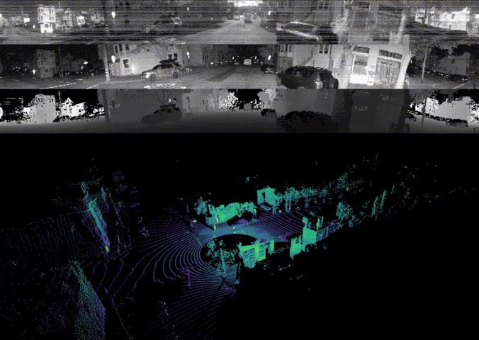
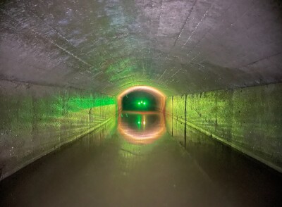
Ambient data at top, depth data at bottom, gathered simultaneously by one Ouster lidar.
Hopes and speculation
When I caught up with a few 3D-tech veterans to hash out the consequences of this technology, a few speculated that VCSEL-based lidar like Ouster’s could be a “game-changer” for the handheld 3D-capture market once it shows up in 2D arrays (currently, Ouster builds 1D arrays that they spin to achieve coverage of a scene).
One of my contacts speculated that if you could put a 2D array with thousands of these VCSELs on a low-cost, low-power, and light-weight chip, you could come close to the long-held dream of a “credit-card sizes lidar sensor that could be slapped onto any surface.” That means high-quality 3D scanning anywhere, the kind of ease of capture hinted at by Apple’s 3D depth camera/face sensor. He also wondered if it could be possible to combine data from a number of VCSEL chips, each one configured to sense a different defined range, or particular bands of light (thermal, RGB, etc) to offer the equivalent of multi-sensor capabilities in a small package.
A common sentiment in my conversations: 3D tech is overdue for a sea change, and VCSEL-based technology like Ouster’s represents a chance to get away from the spinning mirror and finally go solid-state. Of course, time will tell, and most are waiting to get their hands on the technology before they make up their minds about the potential.
For more information about Ouster’s lidar, I recommend checking out other SPAR articles, especially our article about Ouster’s ability to capture ambient data without a camera, and what that means for AI, SLAM, and sensor fusion problems. After that, dig into CEO Angus Pacala’s blog post here, and getting in touch with Ouster through their official website.